Preface:
Below is a general overview of the silicon wafer characterization project. Technical details can be found in: Nondestructive PE characterization of mc-Si PV wafers.Introduction:
Monocrystalline and multicrystalline silicon solar cells make up over 90% of the world's solar cells in terms of cumulative installed capacity. An important building block for each solar cell is a silicon photovoltaic (PV) wafer.
The photovoltaic wafers are sliced from silicon ingots with a wiresaw. The wire sawing process creates many microscopic cracks on the surface of the wafer which are referred to as saw damage. Microcracks have an adverse effect on solar cell efficiency and wafer strength. Because silicon is a brittle material, the distirbution of cracks in a silicon wafer determine it's strength, as soon as any microcrack begins to propagate the wafer will fracture.

The majority of these microcracks reside near the wafer’s surface and thus many of them can be removed through steps such as etching which removes a few microns of material from the top and bottom surfaces of the wafer. This increases both the strength and efficiency of the solar cell.
However, etching does not remove all of the microcracks. Between 5 and 15 percent of wafers fracture during the solar cell fabrication process resulting in down time while the wafer shards are removed. The motivation behind this project is to detect wafers that are likely to fracture early in the solar cell fabrication process so that they can be isolated and recycled before they enter the fabrication process.
Approach:
Microcracks adversely affect the strength of silicon wafers and are the root cause of wafer fracture. By measuring the distribution of microcracks on a wafer and the characteristics of each microcrack, informed predictions can be made about a wafer’s strength.This challenge can be broken down into five subproblems:
- Image a single microcrack using infrared polariscopy.
- Scale to image all microcracks on a wafer.
- Identify microcracks within an image via machine learning.
- Characterize a single microcrack by comparing theoretical and measured crack tip stress fields.
- Make informed predictions about each wafer’s strength.
1. Image a single microcrack:
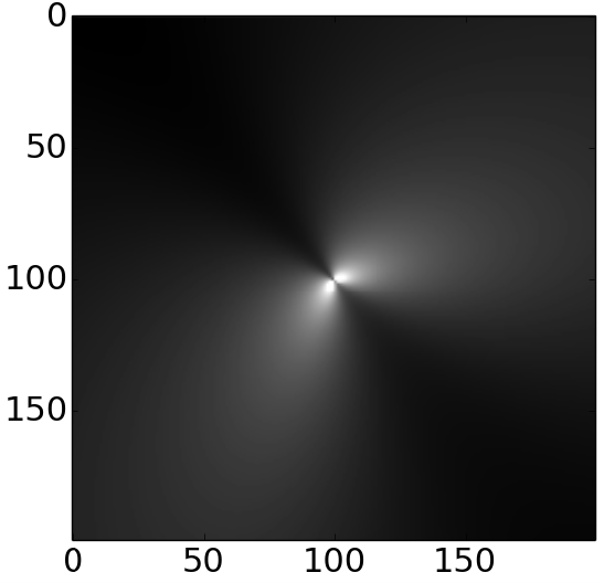
Critical microcracks are on the order of 10μm in length and are much thinner in width. This makes them difficult to detect even under an electron microscope. However, leveraging the photoelastic behavior of silicon and characteristic stress field of a crack tip, microcracks can be detected using photoelastic imaging.
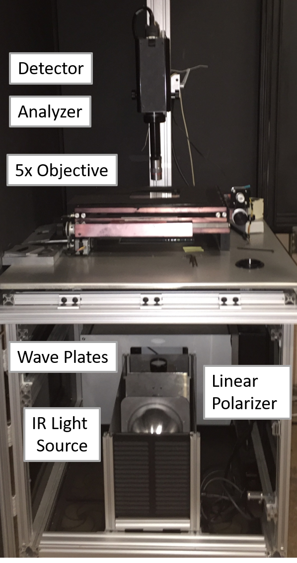
A grey-field polariscope (GFP) is used to measure the residual stress field of silicon wafers. The GFP must be able to pass circularly polarized light through the silicon wafer so it uses an infrared (IR) light source since silicon is transparent to IR light. Furthermore, in order to resolve the locally elevated stress fields caused by cracks, the IR-GFP is fitted with a 5x microscope objective lens.
With the above modifications, the IR-GFP is capable of detecting the locally elevated stress fields around microcracks. These locally elevated stress fields appear as bow-tie patterns in the IR-GFP images.
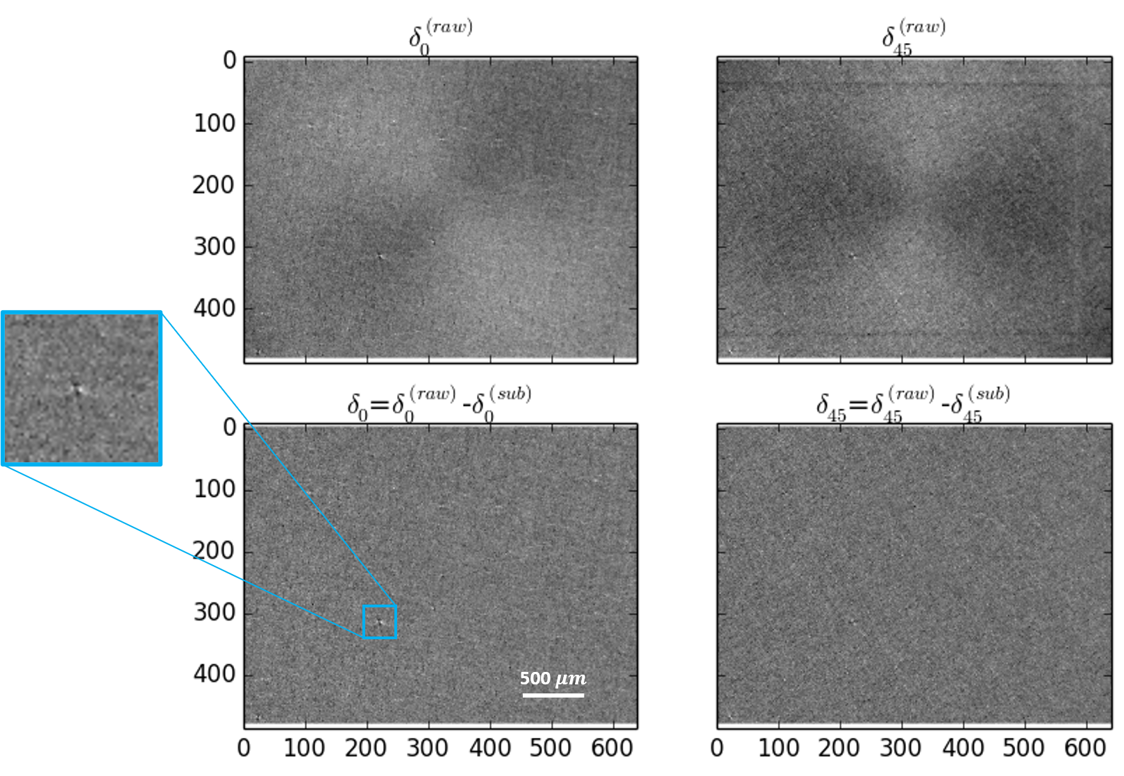
Raw images are often obscured by artifacts due to imperfections in the detector and optic path, internal reflections, and dust particles. Post processing steps such the application of subtraction images and identification of hypersensitive pixels are taken to clean up the raw image data.
2. Scale to image all microcracks on a wafer
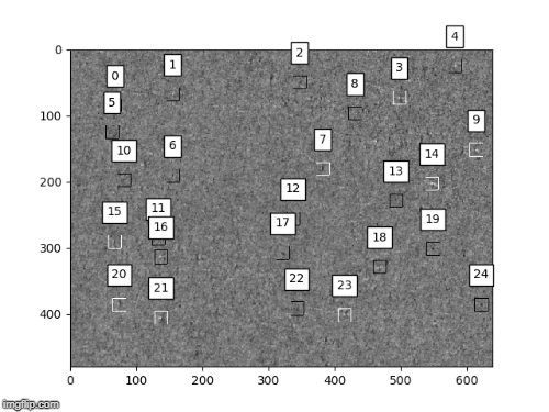
The addition of a microscope objective to the IR-GFP setup increases the system’s resolution enough to detect micro-crack stress fields, however it limits the field of view to a 2.4 by 3.2 mm region. As such, over 3,000 images are required to cover the entire wafer’s area. To address this the x-y stage that the silicon wafer rests on was retrofitted with stepper motors controlled by an Arduino. The Arduino is programmed to work in sync with the IR-GFP imaging software such that the detector will take a 5x IR-GFP image and while the image is being saved, the stepper motors will move the x-y stage to the next imaging position.3. Identify microcracks within an image
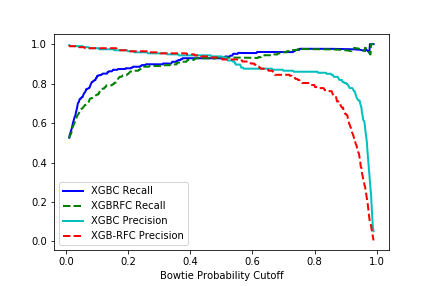
Rather than manually identifying and recording all bowtie features in 3,000 images for 18 wafers, a sample of 963 bowtie and 963 non-bowtie 40 by 40 pixel image regions were manually extracted from the post-processed images. Several machine learning classifiers were trained on both the training data and a line scan swept around the bowtie separately. A detailed explanation of the ML model training and model selection process can be found in Bowtie Defect Identification. Extra Trees (ET), Random Forest (RF), Support Vector Machine (SVM), and Extreme Gradient Boosted (XGB) classifiers were trained on the full image and circle sweep data. The highest performing model was the extreme gradient boosted classifier achieving an F1 score of 0.913.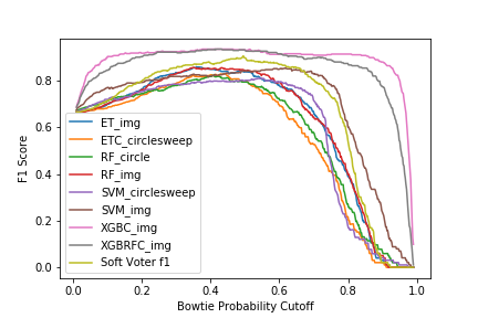
4. Characterize a single microcrack
The next step is to analyze each crack tip stress field in order to determine the crack’s orientation and stress intensity factors. This is accomplished by fitting the measured crack tip retardation profile (IR-GFP bowtie image) to the theoretical crack tip retardation profile (calculated from linear elastic fracture mechanics principals). Technical details of the fitting process are described here.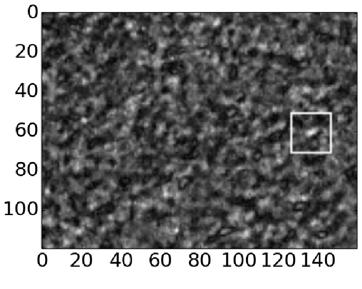
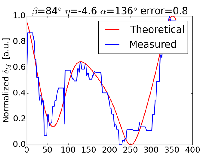
If the best fit theoretical retardation profile is a low quality fit - quantified by MSE - then the region will be omitted from the list microcracks. In this way the fitting process acts as a secondary filter to remove non-bowties.
5. Predict the strength of each wafer
A linear relationship exists between the tensile stress normal to a crack’s plane and a crack’s mode I stress intensity factor (KI). When KI equals the material’s critical stress intensity factor (KIC), also known as the fracture toughness, then the crack will propagate. Since silicon is a brittle material, as soon as a crack begins to propagate under a tensile load the wafer will catastrophically fracture. Having derived the relationship between KI and the stress normal to the crack plane σ⊥ in step 4. The applied tensile load required to cause each microcrack to propagate is calculated and the predicted strength of the wafer under a tensile load is the applied tensile load that will cause the first crack to propagate.The predicted strength of each wafer in the wafer group can be used as a characteristic by which weak wafers can be filtered out prior to the solar cell fabrication process. Finally, because the wafer strength calculation uses a virtually applied load, this technique could feasibly be extended towards characterizing the strength of wafers under other stress distributions such as wafer handling or a Bernoulli Gripper.