band-to-band-PL-analysis
This repository contains a study of the band-to-band (BB) photoluminescence (PL) images from 8 regions of a fractured multicrystalline silicon PV wafer that has an antireflection (AR) coating on one side. The experimental setup used to obtain the BB-PL images is described in chapter 4 of Dr. Tung-wei Lin's dissertation. Below, the imaging regions are numbered on said ARC mc-Si wafer.
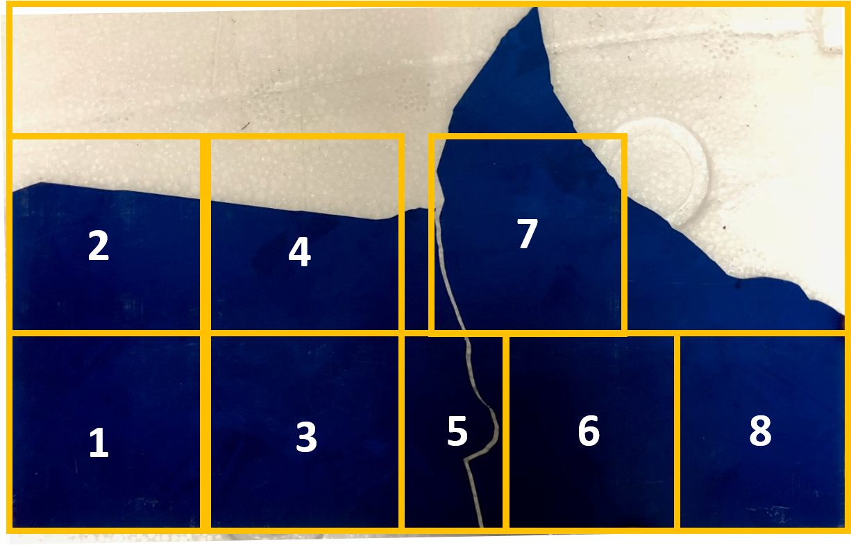
The band-to-band images, shown below, vary in intensity spatially depending on the density of defects. Locations with higher defect densities will appear dark in the BB-PL images because free carriers recombine and weakly emit light at a different wavelength (the defect band wavelength). For this reason, BB-PL images are used to determine the density of defects within a silicon wafer and furthermore estimate the quality of the wafer which is proportional to the defect density. (See alt text for region number)


It is known that defect band PL is polarized; this is discussed in Dr. Lin's disseration. On the other hand, band-to-band PL is unpolarized when emitted. However in this study, we observed a small degree of polarization from BB-PL, ranging between 0 and 5 percent across the wafer, that is constant across any single grain.


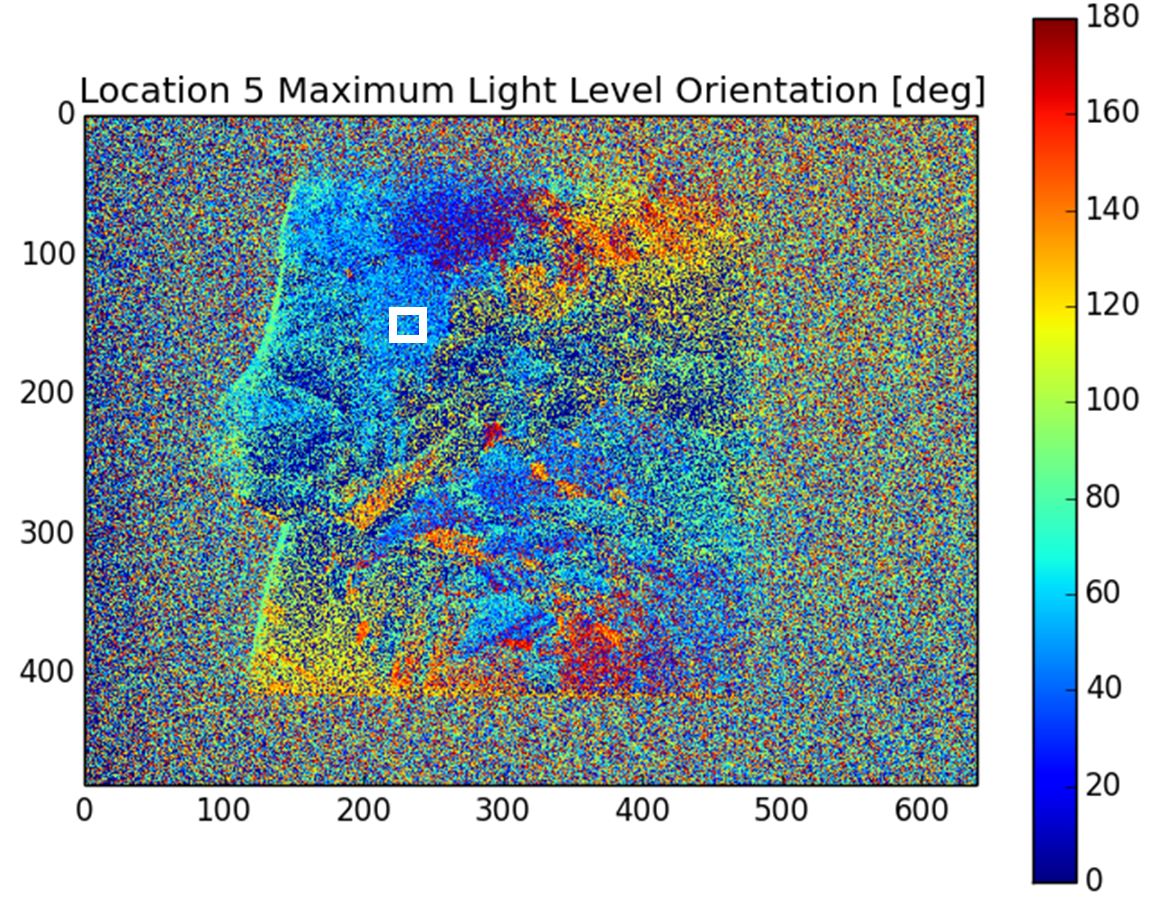
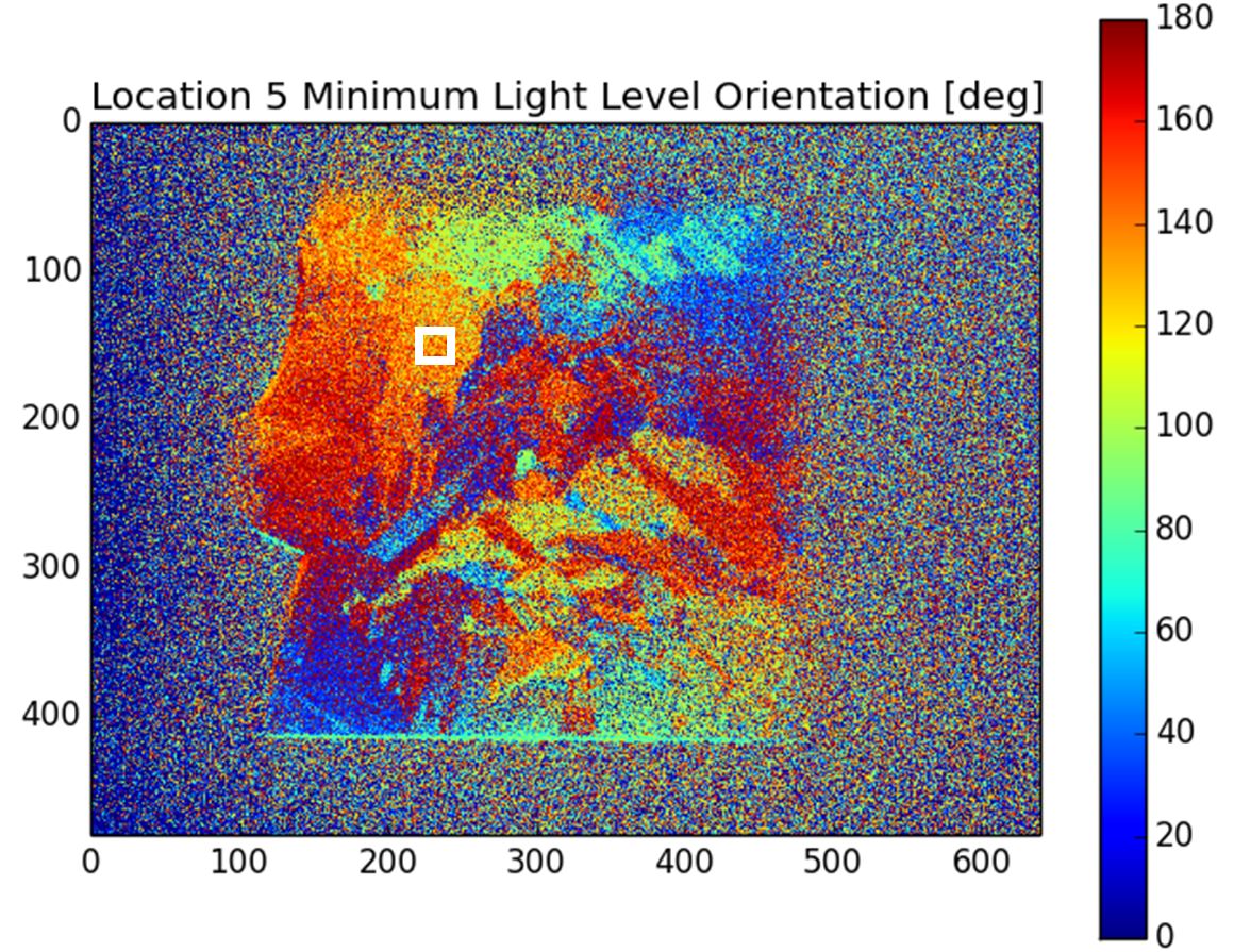
Furthermore, the orientation of the IR-GFP's analyzer at which minimum and maximum intensity of BB-PL occurred also varies across the wafer, yet is constant across grain-like regions.


discussion-of-results
The first question that comes to mind is, "where does the polarization come from?"
It is not a product of the excitation source. We know this because light images 2, 4, 5, 6, and 7 do not fill the entire masked imaging area. Beyond the crisp edges of the broken wafer, the detector is looking directly at the excitation source. It is clear that K5 glass completely absorbs all of the light from the excitation source that would have been visible to the IR-GFP's detector. Thus all of the observed light is emitted from the silicon wafer.
It is not a product of the optic path or the detector since the DoP varies with the wafer's grains.
This leaves two - not necessarily mutually exclusive - possibilities that I believe warrant further exploration.
The silicon has a dichroic axis such that when light's TE component is oriented paralell to the dichroic axis it will be absorbed more strongly than when oriented transverse to the dichroic axis. Silicon can gain dichroic absorption properties due to the manner in which oxygen atoms situate themselves in the silicon matrix.
The etchant used on the wafer surface affected each grain differently based on the crystal orientation. Thus when light (originating as unpolarized within the wafer) is transmitted across the silicon-air interface, the light becomes slightly polarized due to partial internal reflections that occur the textured surface.
The contribution to the polarization of the BB-PL light due to dichroic absorption and transmission across an etched surface can be determined experimentally. First measure the degree and orientation of polarization of the BB-PL light from a polished mc-Si silicon wafer. Preferably use a laser excitation source as opposed to our in-house LED excitation source that requires one side of the wafer to be AR coated. Use an SEM to determine the crystal orientation of each grain. Etch the wafer and repeat the PL imaging process to measure degree and orientation of polarization. Finally, check whether the grains are visible in the DoP image before etching, after etching, and if the DoP image was altered by the etching process.
Due to the consistent nature of the degree of polarization and polarization direction of BB-PL across individual grains, it may be possible to determine grain orientation in multicrystalline silicon wafers from band-to-band PL images. The relation between the PL measurements and grain orientation may be determined by comparing the degree and orientation of polarized PL measurements to the inverse pole figures obtained from the SEM.
data-collection
Using the experimental BB-PL imaging setup described in chapter 4 of Dr. Tung-wei Lin's dissertation, turn on the IR-GFP (with lens cover on) and the LED light source and allow a few minutes for both to reach thermal equilibrium.
Place the ARC mc-Si wafer ARC side down (facing the excitation source) on the metal support stage. Disable rotation of the IR-GFP analyzer and set the number of rotations to 10. This effectively takes 16x10=160 images with the analyzer locked in the same position. You may also wish to increase the gain and reduce the noise filter at this time since the resulting BB-PL will be low intensity.
Save a BB-PL image when the analyzer is at 0°, increase the analyzer position by 10° and save another BB-PL image. Repeat this process until the analyzer has spanned 180°. This process will then be repeated for each area of interest on the wafer.
analysis
In this section I will briefly discuss each script in the repository in the order they are inteded to be run.
1. Convert the raw data into light arrays.
The raw data for location 1 is stored in data/1. It consists of 19 BB-PL images at analyzer angles incremented by 10 from 0 to 180. [1_extract_light_levels_from_data.py] creates a (19,480,640) array for each image location where each of the 19 layers is a BB-PL image for a different analyzer angle. The "light array" for location 1 is saved as light-arrays/1_LightArray.npy.
2. Calculate the degree of polarization and orientation of the polarization
Both [2_DoP...] scripts perform the same function using different inputs. On a pixel by pixel basis, script 2 will find the analyzer orientation at which BB-PL intensity was maximum (omax), minimum (omin), and the degree of polarization (dop). A truncation value (tval) is set to 6% to improve dop image contrast. This is necessary since regions off the wafer - where the BB-PL image is just noise - return very high dop values.
Degree of polarization is calculated as (max - min)/max where referring to the maximum (minimum) intensity of a given pixel at any of the 19 analyzer angles.
3. Calculate the difference in angle between omax and omin
This is not a necessary step, but it does contain unexpected results. omax (omin) is the orientation of the analyzer at which the intensity of a pixel is at its maximum (minimum). In the case of linear or elliptic polarization, regardless of purity, one would expect to see the angle between the max and min intensities to be 90°. However as shown below, this is not always the case.


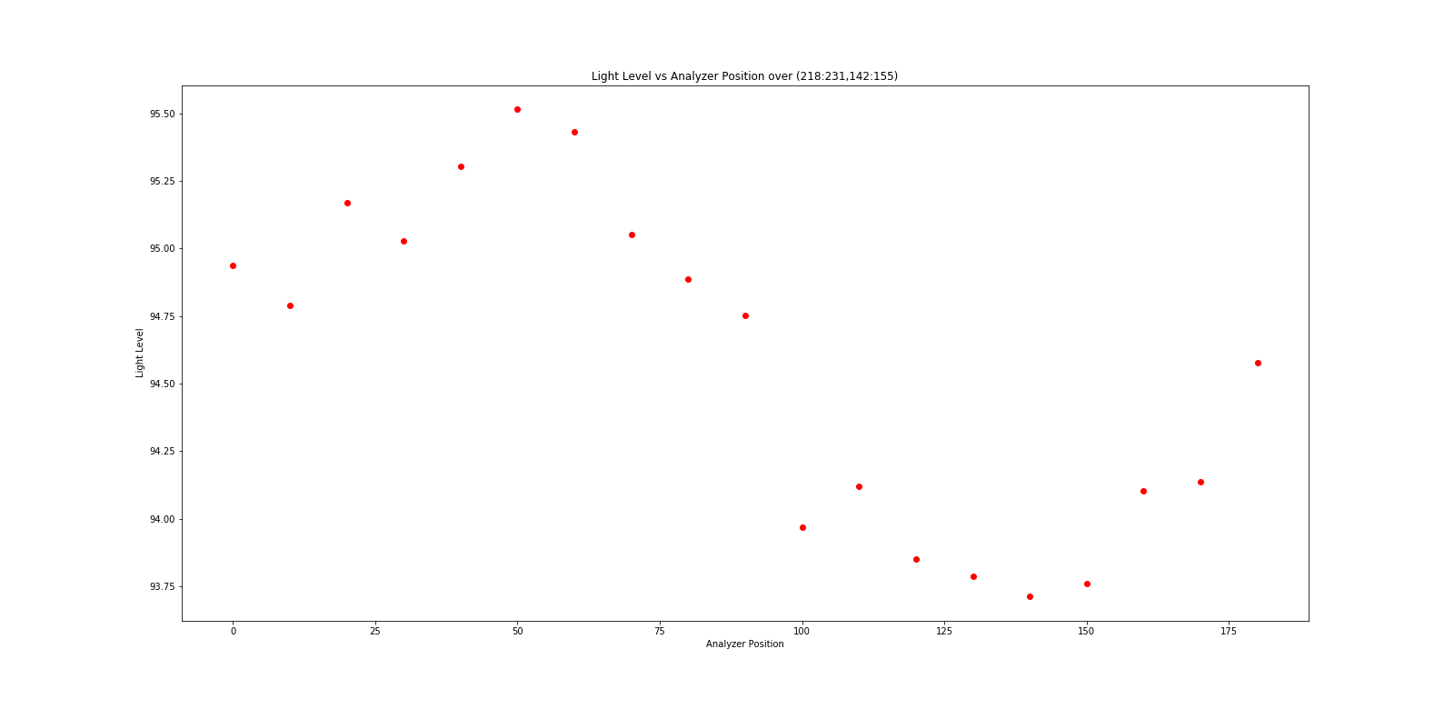
However, take this specific observation with a grain of salt because the degree of polarization measurements had the occasional anomaly at the analyzer ange of 0°. This is evident in the next section when plotting the polarization ellipse for specific grains.
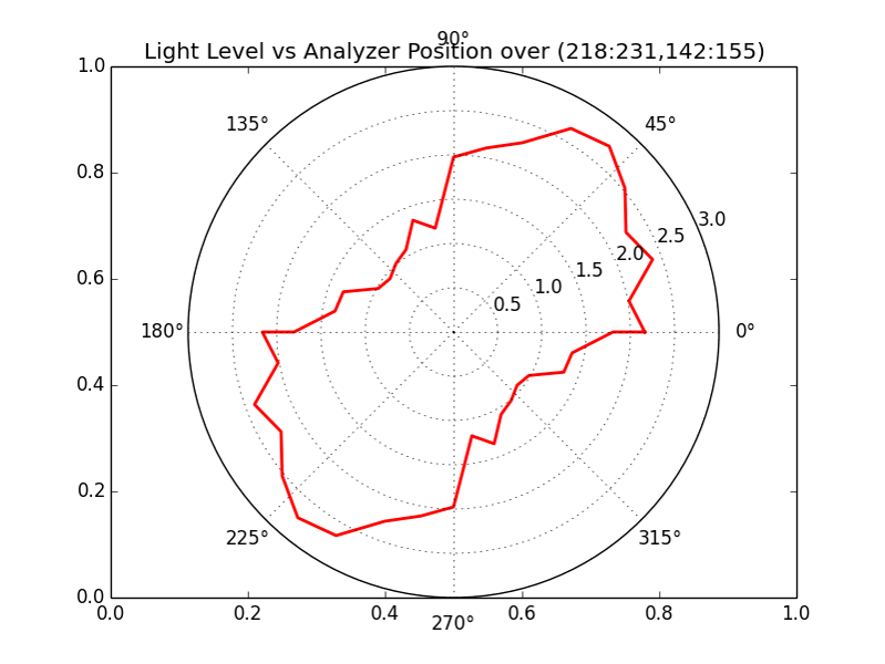
4. Plot the polarization ellipse
[5_light_level_vs_analyzer_angle_polar_plot.py] Takes an input of the image location and rectangular region of interest. It will return a polarization ellipse consiting of the average intensity at each analyzer position for the pixels contained within the region. An example is shown below for location 5 in the region of x=218..231 and y=142..155.
5. Calculate the azimuthal and polar angle of the dichroic axis for each Si grain
Now look at the BB-PL polarization ellipse above and let us assume that the polarization is caused by dichroic absorption in the silicon where light is absorbed more strongly when its TE component is aligned with the dichroic axis. This would tell us that the projection of the dichroic axis on the wafer surface is 135° from the x+ axis of the detector. This is because it is along that direction that the BB-PL signal was the weakest. We will call this the dichroic axis' azimuthal angle, ψ.
Using the same assumption regarding the dichroic axis, the degree of polarization would be at a maximum (minimum) when the dichroic axis is oriented parallel (orthogonal) to the wafer surface. Thus, we can use the minimum and maximum measured DoP across all grains to bound the polar angle (θ) of the dichroic axis. From these bounds we can interpolate to find the polar angle of the dichroic axis of any grain based on the grains BB-PL degree of polarization.
Below the polar and azimuthal angle are depicted where z+ is normal to the wafer surface.
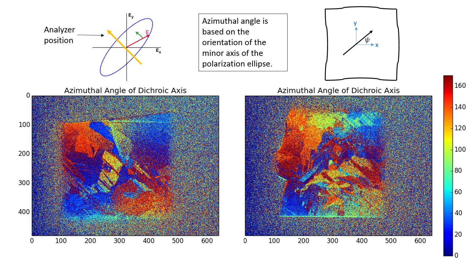
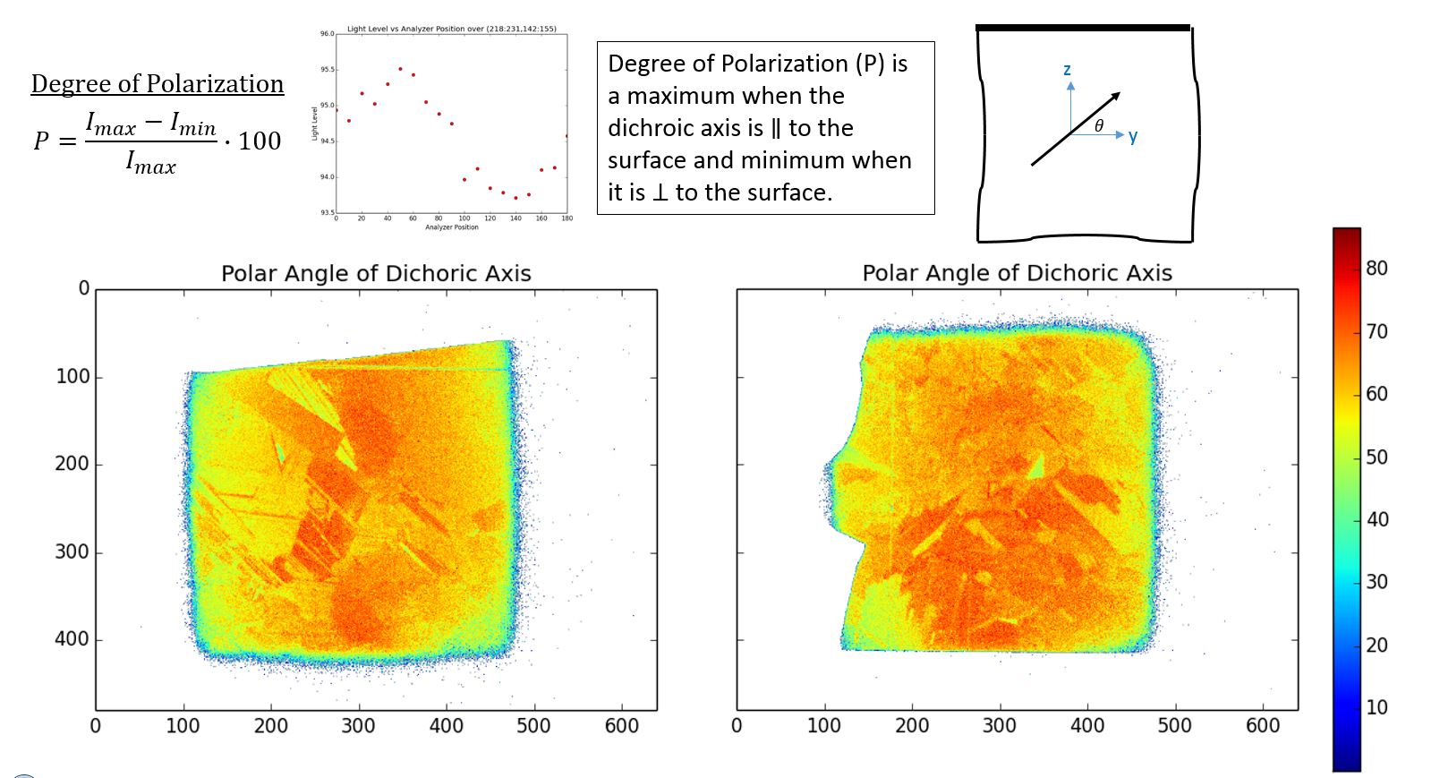
Please see the description within the header of script [4_polar_and_azimuthal_orientation_plots.py] to better understand how the values in the above images were computed.
6. Generate average intensity BB-PL images for each location
[6_investigate_ave_light_intensity.py] is an additional script included only for convenience. It simply outputs the average light image of 19 BB-PL images for each location.
closing-remarks
The observations made in this project suggest that there is an underlying cause responsible for the polarization observed in BB-PL measurements.
Gaining an understanding of this cause, possibly through the proposed methods above, may aid in the the determination of multicrystalline silicon grain orientations from band to band photolumnescence measurements.
Among other benefits, knowledge of each grains orientation would allow for more accurate infrared PE stress analyses of multicrystalline silicon wafers.