3D-nanopore-reconstruction
In this project, the formation and shrinkage of nanopores was studied in Si3N4 membranes using a Ga+ ion beam and scanning electron beam respectively. The purpose was to observe the shape of nanopores as they formed. To do so nanopores were imaged at various stages of opening via a backscattered electron (BSE) detector in a dual-beam FIB/SEM. From the 2D SEM images, 3D images of the nanopores were reconstructed.
Brief Summary
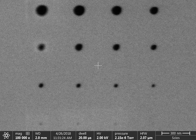
Initial tests (and the SCIOS 2 FIB/SEM documentation) suggest that 1.5 pA current and 30 keV accelerating voltage are the optimal settings for FIB milling small nanopores. Several arrays similar to the one below were milled with a two-fold purpose. First to determine the minimum exposure time necessary to create a nanopore and second to study how the shape of a nanopore evolves under Ga+ irradiation.
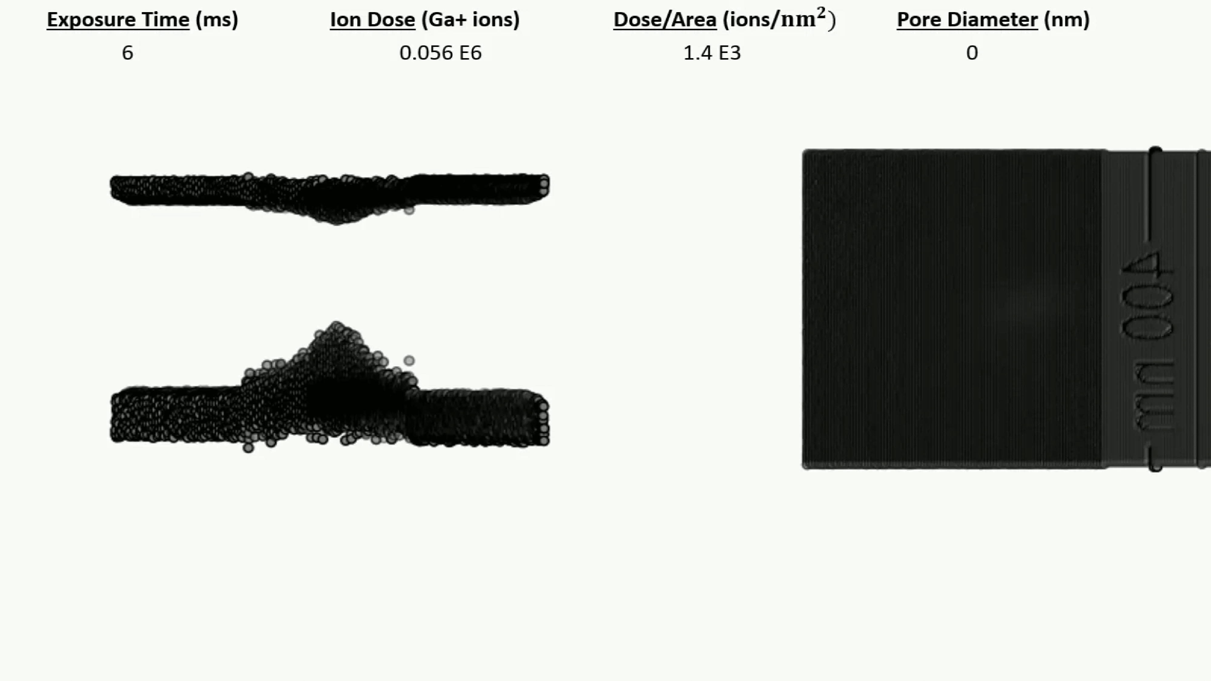
The 3D reconstruction process was performed for all of the nanopores in an array piror to and post pore formation. A GIF of 18 nanopores at various stages of opening is shown below.
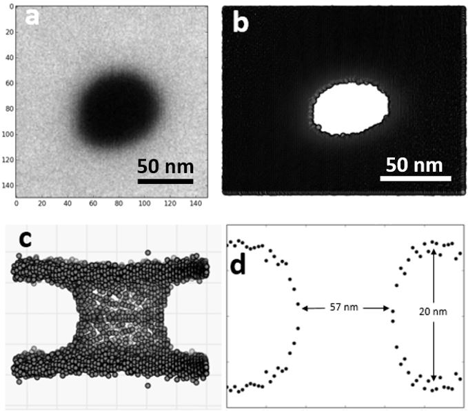
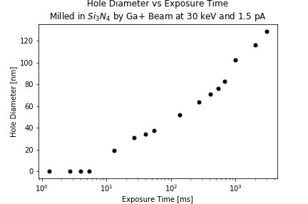
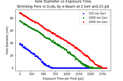
The diameter of each nanopore was calculated by counting the total number of pixels contained within the pore and assuming that the pore is approximately circular in shape. The diameter of each pore was plotted versus the Ga+ exposure time used to form the nanopore.
The nanopores formed by Ga+ exposure will shrink under electron irradiation (see below).
<-- Before & After -->


Every time a SEM image was taken, each pixel was exposed to a 25pA at 2keV electron beam for 10 μs. The diameters of the pores were measured in each image and plotted versus the total e-beam exposure.
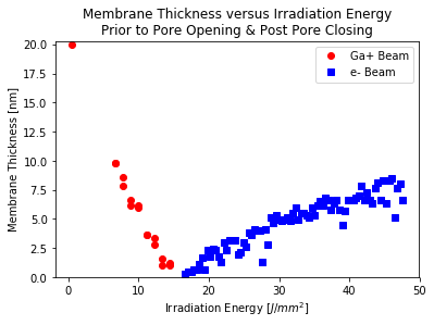
Finally, thickness measurements at the center of nanopores were made prior to the pore opening due to Ga+ irradiation and after the pore had closed due to electron irradiation. Since the thinning process is caused by a Ga+ source with a Gaussian distributed and the healing process is caused by an electron source that is raster scanned across the imaged region, the most convenient way to compare the irradiation dose is in J/mm. The rate of membrane thinning and healing can be observed below.
This project was carried out in part in the Materials Research Laboratory Central Research Facilities, University of Illinois